Table of contents
2 inch (approximately 50.8 millimeters) sapphire wafers are small circular discs made of sapphire, a crystalline form of aluminum oxide (Al2O3). These wafers are commonly used in various applications in the semiconductor industry, including the production of LEDs, integrated circuits, and other electronic devices.
Sapphire wafers are valued for their high thermal conductivity, optical transparency, and resistance to chemical and mechanical damage, making them ideal substrates for manufacturing processes that require precision and durability.
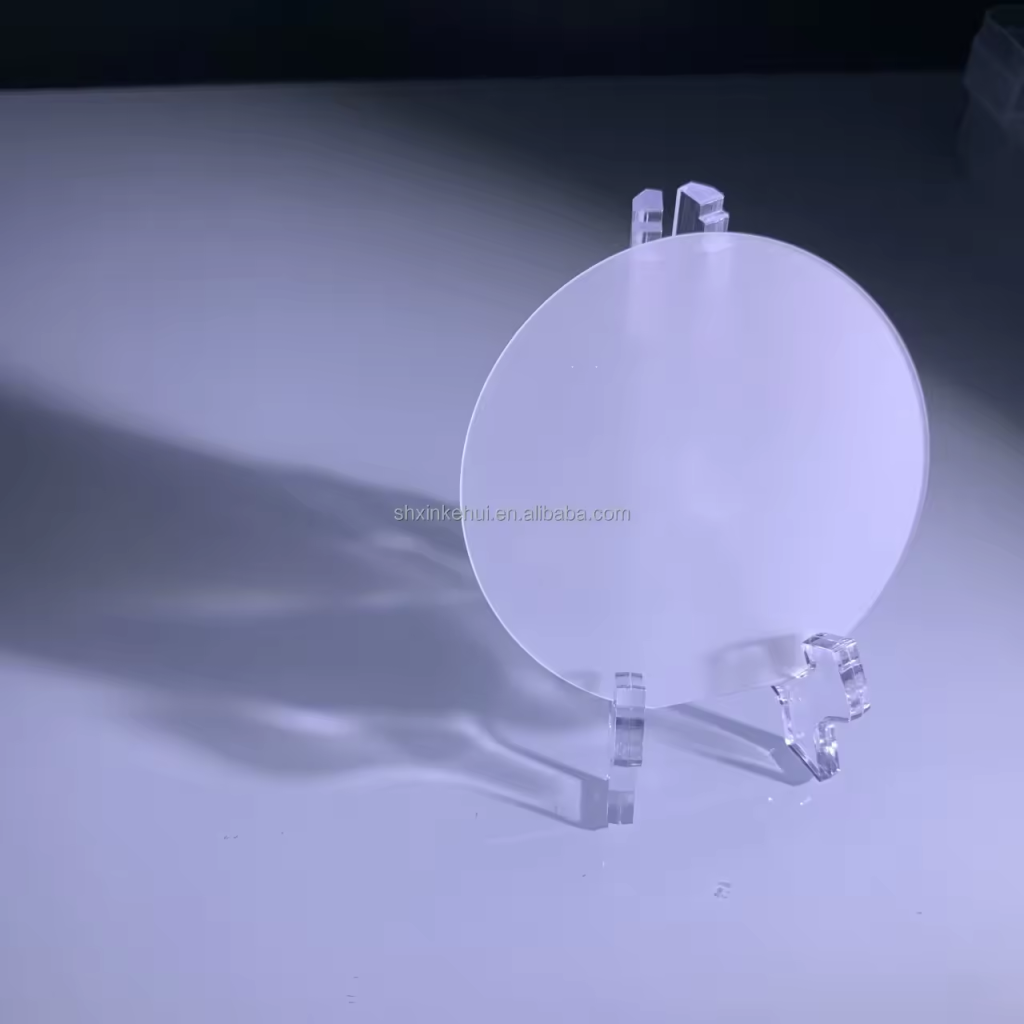

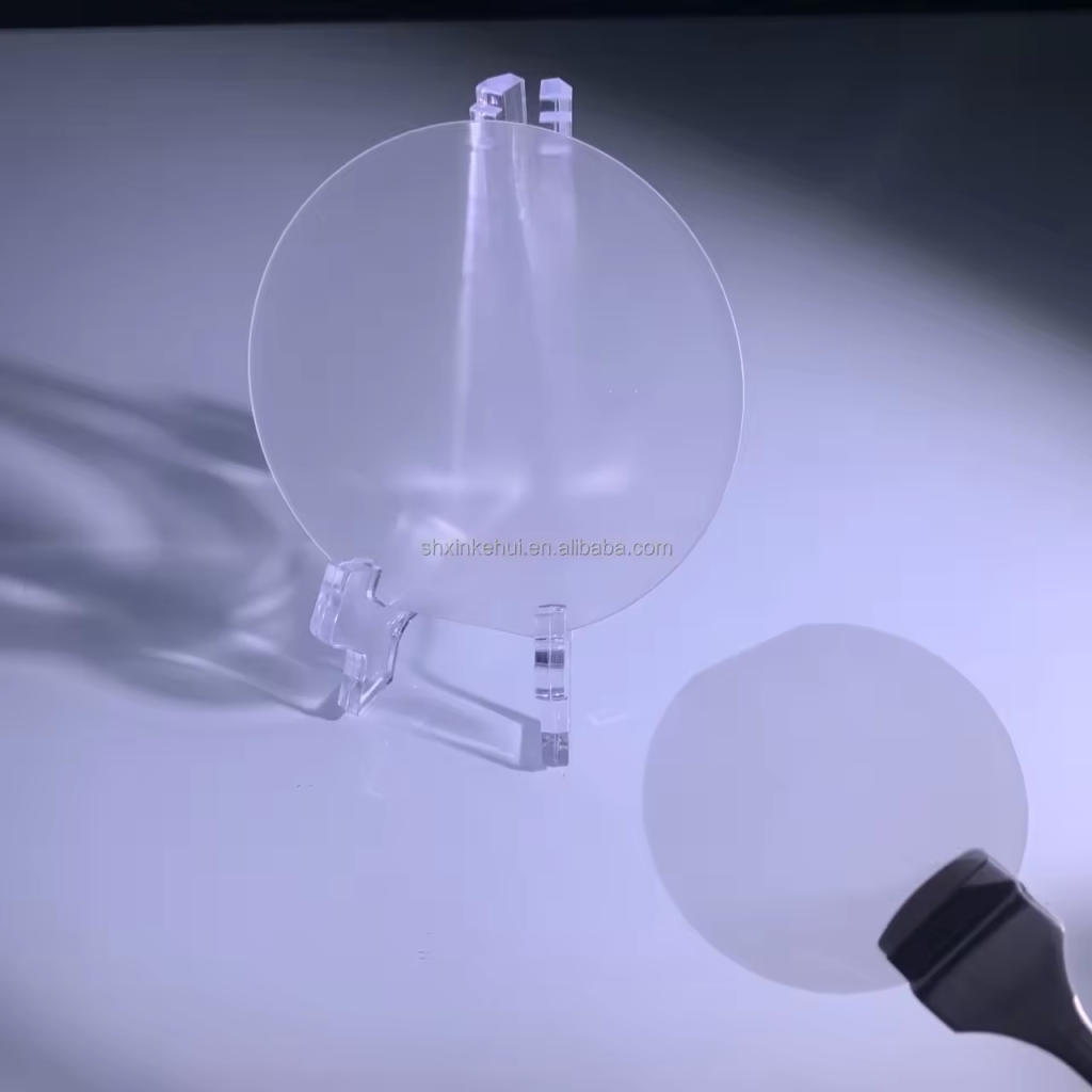
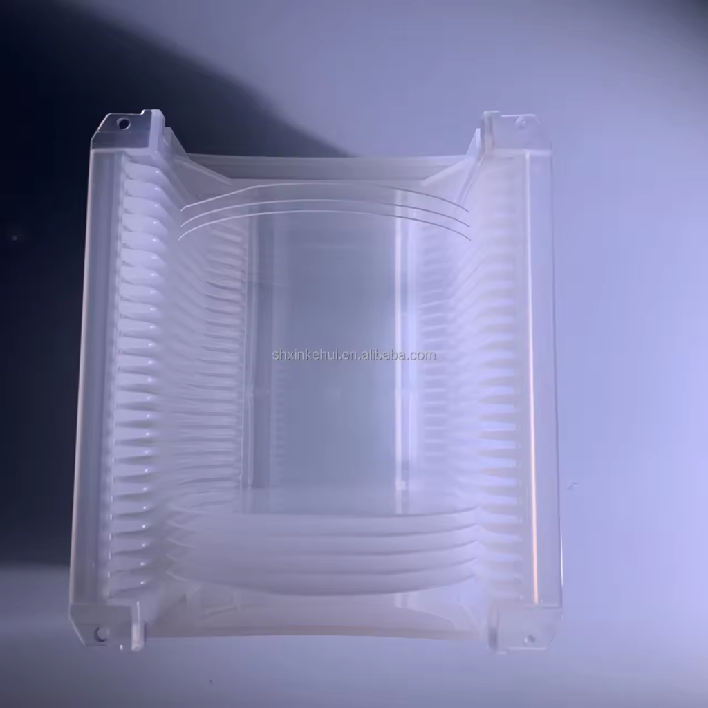
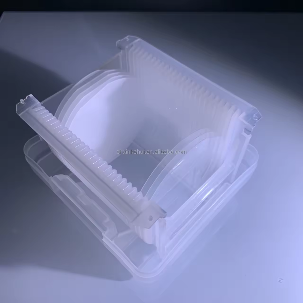
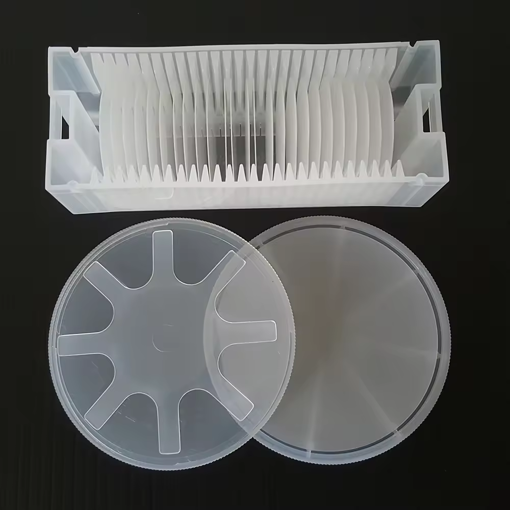
1. Excellent Hardness: 2 inch sapphire wafers possess extraordinary hardness, second only to diamond on the Mohs scale. This characteristic ensures outstanding resistance to scratching, abrasion, and wear, making it an ideal material for harsh environments.
2. High Thermal Conductivity: The thermal conductivity of 2 inch sapphire wafers exceeds that of most other substrate materials, facilitating efficient heat dissipation and ensuring optimal performance and reliability in high-temperature applications.
3. Optical Transparency: Transparency across a broad wavelength range from ultraviolet to near-infrared endows 2 inch sapphire wafers with invaluable value in optical and optoelectronic applications (including LEDs, laser systems, and optical windows).
4. Chemical Inertness: 2 inch sapphire exhibits excellent resistance to chemical corrosion, remaining unaffected by acids, alkalis, and other aggressive chemicals. This property enhances the lifespan and reliability of devices utilizing sapphire wafers in chemically corrosive environments.
5. Mechanical Stability: The inherent strength and rigidity of 2 inch sapphire contribute to its mechanical stability, ensuring crucial dimensional accuracy and uniformity in semiconductor manufacturing processes.
2 inch sapphire wafers are widely used in many industries, some of the major industries include:
1. LED production: Sapphire wafers are used in LED manufacturing as substrates for the epitaxial growth of gallium nitride (GaN) layers, helping to produce high-brightness, energy-efficient lighting solutions for a variety of applications including displays, automotive lighting and general lighting. .
2. Semiconductor devices: In the semiconductor industry, sapphire wafers are used as substrates for manufacturing high-frequency, high-power devices such as radio frequency (RF) amplifiers, microwave integrated circuits (MICs), and power semiconductor devices.
3. Optoelectronics: Due to its optical transparency and mechanical durability, sapphire wafers are used in the production of optical components, including lenses, windows and prisms, as well as in the manufacture of photonic devices such as laser diodes and optical sensors.
4. MEMS and sensor technologies: Sapphire wafers are chemically inert, biocompatible, and have the ability to withstand harsh operating conditions, making them an excellent platform for manufacturing microelectromechanical systems (MEMS) and sensors.




| Specification Parameter | 2 inch |
| Diameter | 50.8± 0.1 mm |
| Thickness | 430±15 μm |
| Surface Roughness | Ra ≤ 0.3 μm |
| Warpage | ≤ 10 μm |
| Total Thickness Variation | ≤ 3 μm |
| Surface Quality | 20/10 |
| Surface Condition | Double-sided polished or Single-sided polished |
| Shape | Circular or with orientation Flat |
| Chamfer | 45°, C Shape |
| Material | Sapphire Crystal |
| Note | Sapphire wafers are customizable |