Table of contents
A 6 inch sapphire wafer refers to a circular thin slice of sapphire crystal with a diameter of approximately 6 inches (about 152.4 millimeters). These wafers are commonly used in the manufacturing of semiconductor and optoelectronic devices. Sapphire wafers possess excellent optical and physical properties such as high transparency, hardness, and chemical inertness, making them widely utilized in various high-end applications.
During the fabrication process, sapphire wafers are typically produced through a series of steps including the growth, cutting, and polishing of sapphire crystals. These steps require highly skilled techniques and precise equipment to ensure the quality and performance of the wafers meet the requirements.
The size and characteristics of 6 inch sapphire wafers make them ideal substrate materials for devices such as LEDs, laser diodes, optical windows, and more. They can withstand high temperatures and chemical corrosion while maintaining stable optical performance, making them well-suited for use in demanding applications.
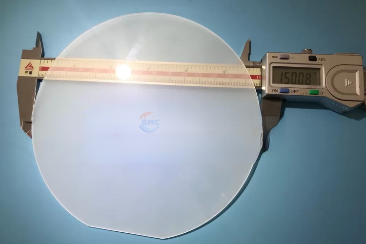

6 inch sapphire wafers, with their outstanding optical and physical properties, hold significant importance in various high-end applications, playing a crucial role in both the optoelectronics and semiconductor fields. Here are the advantages of 6 inch sapphire wafers:
1. High Transparency: Sapphire wafers exhibit exceptional optical transparency, capable of transmitting both visible and infrared light, making them suitable for numerous optical applications.
2. High Hardness: Sapphire ranks as the third hardest natural material in the world, following diamond and boron nitride. This attribute provides sapphire wafers with excellent resistance to abrasion and scratching.
3. Chemical Inertness: Sapphire demonstrates good resistance to a wide range of chemical substances, including acids and alkalis, making it excel in harsh environments.
4. Stability: The crystal structure of sapphire wafers is highly stable, possessing excellent thermal stability and mechanical integrity, even under high temperature and pressure conditions.
5. Wide Range of Applications: 6 inch sapphire wafers find applications in the manufacturing of LEDs, laser diodes, optical windows, semiconductor substrates, and more, extensively utilized across the fields of optoelectronics, semiconductors, and optics.
6. Advantage of Large Size: With a diameter of 6 inches, these wafers offer the advantage of larger size, contributing to enhanced production efficiency and cost-effectiveness in device manufacturing processes.
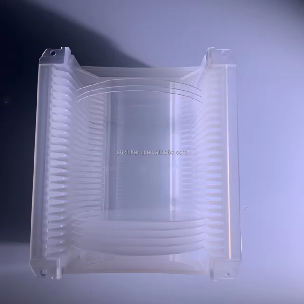
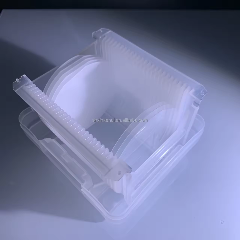
6 inch sapphire wafers have a wide range of applications across various industries, including:
1. Optoelectronics Industry: Sapphire wafers are used to manufacture LED (Light-Emitting Diodes), laser diodes, optical windows, and other optoelectronic devices. LEDs are crucial components in the lighting industry, while laser diodes find applications in laser printers, fiber optics communications, laser cutting, and more.
2. Semiconductor Industry: In semiconductor manufacturing, sapphire wafers can serve as substrates for growing other semiconductor materials such as gallium nitride (GaN). These substrates are often used in the production of high-performance power electronic devices and optoelectronic devices.
3. Optics Industry: Due to their excellent optical transparency and chemical stability, sapphire wafers are utilized in the production of optical windows, lenses, prisms, and other optical components. These components are widely used in laser systems, optical instruments, cameras, and more.
4. Consumer Electronics Industry: Sapphire wafers are also employed in manufacturing screen protectors for electronic devices such as smartphones, tablets, digital cameras, and other consumer electronics. Their high hardness and scratch resistance help protect displays from damage.
5. Aerospace Industry: In the aerospace sector, sapphire wafers are used to manufacture high-performance optical sensors, windows, turbine engine nozzles, and other components to meet stringent environmental and performance requirements.


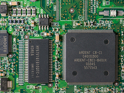

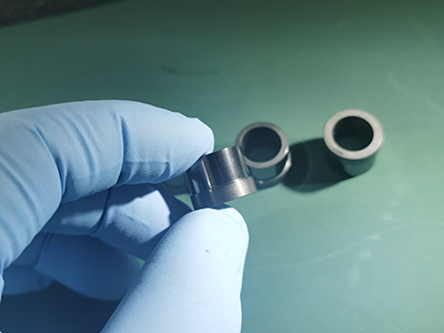

These applications highlight the versatility and importance of 6 inch sapphire wafers in various cutting-edge industries.
| Specification Parameter | 6 Inch |
| Diameter | 152.4 ± 0.1 mm |
| Thickness | 1000 ± 25 μm |
| Surface Orientation | C-Plane (0001) tilted M-axis 0.2°/0.35°± 0.1° |
| Primary Flat | A-Axis (11-20) ± 0.2° |
| Orientation Length | 47.5 ± 2.0 mm |
| TTV | < 25 μm |
| Bow | -30 ~ 0 μm |
| Surface Condition | Double-sided polished or Single-sided polished |
| Shape | Circular or with orientation Flat |
| Material | Sapphire Crystal |
| Note | Sapphire wafers are customizable |
The production process of 6 inch sapphire wafers typically involves several main steps:
1. Crystal Growth: The preparation of sapphire wafers usually begins with the growth of sapphire crystals. Various methods such as the Czochralski method, Kyropoulos method, or edge-defined film-fed growth (EFG) method can be employed. In this process, sapphire crystals are grown from molten sapphire by controlling parameters like temperature, pressure, and others.
2. Cutting: The grown sapphire crystal needs to be sliced into thin slices, known as wafers. This is typically achieved using diamond cutting tools to ensure that the cut slices meet the required size and shape.
3. Polishing: After cutting, the surface of the sapphire wafers may have some rough or uneven areas, thus requiring polishing to achieve a smooth surface. Polishing processes may include mechanical polishing, chemical-mechanical polishing (CMP), or electrochemical polishing.
4. Cleaning: The polished sapphire wafers need to undergo thorough cleaning to remove surface residues and contaminants. This usually involves immersion in solvents, ultrasonic cleaning, or other cleaning methods.
5. Quality Inspection: The finished sapphire wafers undergo rigorous quality inspection to ensure they meet specified quality standards. Inspection includes visual inspection, dimension measurement, crystal structure analysis, and more.
6. Packaging and Storage: The sapphire wafers are protected through appropriate packaging to prevent damage or contamination during transportation and storage. Wafers are typically packaged in special boxes or containers and stored in a dry, dust-free environment.

These process steps ensure the production of high-quality, compliant 6 inch sapphire wafers, providing a reliable foundation for their important role in various applications.