Table of contents
A GaN (Gallium Nitride ) wafer is a substrate material used primarily in the production of semiconductors. GaN is a wide bandgap semiconductor material, meaning it can operate at higher voltages, temperatures, and frequencies than traditional silicon-based semiconductors. Here are some key points about GaN wafers:
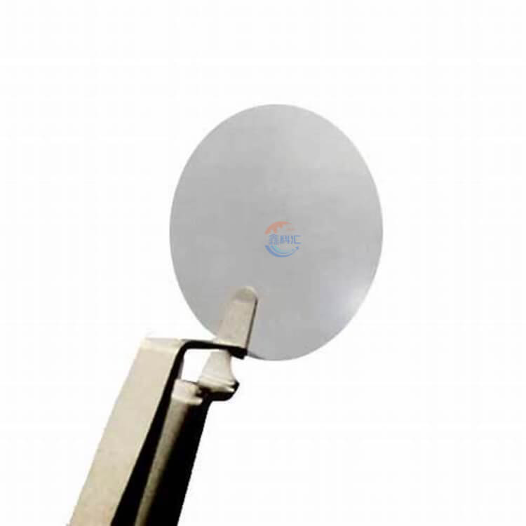
Material Properties:
GaN has a wide bandgap of about 3.4 eV, compared to silicon’s 1.1 eV. This allows GaN devices to function at higher temperatures and voltages, with better efficiency and faster switching speeds.
Applications:
GaN wafers are used in various applications
Power electronics: GaN devices can handle higher power densities, making them suitable for power converters, inverters, and other power management systems.
Radio Frequency (RF) devices: GaN’s high electron mobility makes it ideal for RF amplifiers, especially in telecommunications, radar, and satellite communication systems.
Optoelectronics: GaN is widely used in light-emitting diodes (LEDs), laser diodes, and photodetectors due to its efficiency in emitting blue and ultraviolet light.
Advantages over Silicon
GaN-based devices have several advantages over traditional silicon-based devices
Higher efficiency: Reduced energy loss and better thermal management.
Higher power density: Smaller and lighter devices for the same power output.
Faster switching speeds: Improved performance in high-frequency applications.
Manufacturing:
GaN wafers are typically grown on substrates such as silicon carbide (SiC) or sapphire. The growth process involves techniques like metal-organic chemical vapor deposition (MOCVD) or molecular beam epitaxy (MBE).
Challenges:
Despite its advantages, GaN technology faces challenges such as higher production costs and difficulties in material quality and device reliability.
GaN wafers are revolutionizing many high-performance electronic applications, driving innovation in power electronics, telecommunications, and lighting industries.
Specifications 1
| Items | Values/Scope |
| Substrate | Si |
| Wafer diameter | 4” / 6” / 8” |
| Epi-layer thickness | 4-5 μm |
| Wafer bow | <30 μm, Typical |
| Surface Morphology | RMS<0.5nm in 5×5 μm² |
| Barrier | AlXGa1-XN, 0 |
| Cap layer | In-situ SiN or GaN (D-mode); p-GaN (E-mode) |
| 2DEG density | >9E12/cm2 (20nm Al0.25GaN) |
| >9E12/cm2 (20nm Al0.25GaN) | 1800 cm2/Vs (20nm Al0.25GaN) |
Specifications 2
| Items | Values/Scope |
| Substrate | HR_Si / SiC |
| Wafer diameter | 4’’/6’’ for SiC, 4”/ 6”/ 8” for HR_Si |
| Epi-layer thickness | 2-3 μm |
| Wafer bow | <30 μm, Typical |
| Surface Morphology | RMS<0.5nm in 5×5 μm² |
| Barrier | AlGaN or AlN or InAlN /AlGaN or AlN or InAlN /In-situ SiN or GaN |
GaN wafers offer several advantages over traditional semiconductor materials like silicon, making them highly suitable for various advanced electronic applications. Here are some of the key advantages of GaN wafers:
1. Higher Efficiency: GaN devices have lower on-resistance and higher breakdown voltage compared to silicon devices. This leads to reduced energy losses and higher efficiency, particularly in power conversion applications.
2. High Power Density: GaN can handle higher power levels in smaller sizes, allowing for more compact and lighter devices. This is particularly beneficial for applications like power adapters, electric vehicles, and industrial power supplies.
3. Faster Switching Speeds: GaN transistors can switch at much higher frequencies than silicon transistors. This results in faster data processing and improved performance in RF (radio frequency) and high-speed digital applications.
4. Thermal Management: GaN has better thermal conductivity and can operate at higher temperatures than silicon. This reduces the need for extensive cooling systems and enhances the reliability and longevity of the devices.
5. Wide Bandgap: GaN’s wide bandgap (about 3.4 eV) allows it to function effectively in high-voltage and high-temperature environments. This makes it suitable for applications such as electric vehicles, solar inverters, and aerospace systems.
6. Improved Efficiency in RF Applications: GaN’s high electron mobility and saturation velocity make it ideal for RF and microwave applications, including 5G telecommunications, radar, and satellite communication. GaN RF devices offer higher gain and efficiency compared to their silicon counterparts.
7. Better Performance in High-Frequency Applications: GaN’s ability to operate at higher frequencies makes it suitable for advanced communication systems, where it can provide faster and more reliable signal processing.
8. Enhanced Durability and Reliability: GaN devices exhibit greater resistance to radiation and harsh environmental conditions, making them ideal for aerospace, military, and space applications.
9. Reduction in Size and Weight: The high power density and efficiency of GaN devices allow for smaller and lighter electronic systems, which is beneficial for portable and mobile applications.
10. Cost Savings in the Long Run: While GaN devices may have higher initial costs compared to silicon devices, their superior efficiency and performance can lead to significant cost savings over time due to reduced energy consumption and cooling requirements.

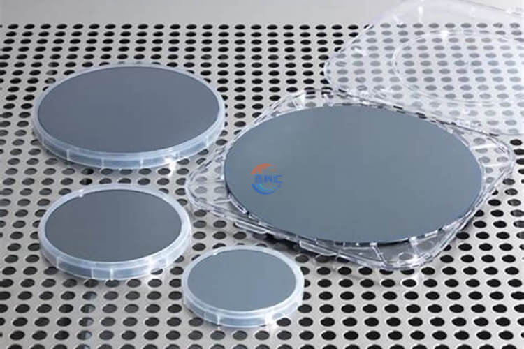

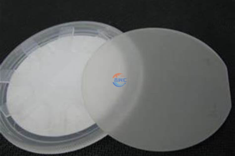


1. RF Power Amplifiers: GaN on Sapphire is widely used in the development of RF power amplifiers for wireless communication systems. Its high-frequency operation and power efficiency make it instrumental in enhancing signal strength in communication networks.
2. Power Electronics: In power electronics applications, GaN on Sapphire is employed for the production of high-performance transistors and converters. Its efficiency and reliability contribute to the advancement of power management systems.
3. LEDs and Lighting: GaN on Sapphire is a key technology in the manufacturing of high-brightness LEDs. Its wide bandgap is well-suited for emitting light in the visible spectrum, making it essential for energy-efficient lighting solutions.
4. Aerospace and Defense: The robustness and reliability of GaN on Sapphire make it suitable for aerospace and defense applications. It is used in radar systems, electronic warfare, and high-frequency communication devices.
5. Automotive Electronics: GaN on Sapphire is increasingly integrated into automotive electronics for power conversion and management. Its ability to operate at high temperatures and handle high power levels aligns with the demanding requirements of automotive applications.


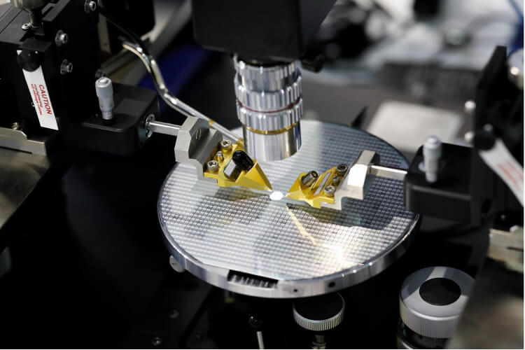
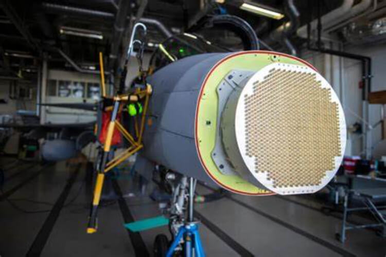
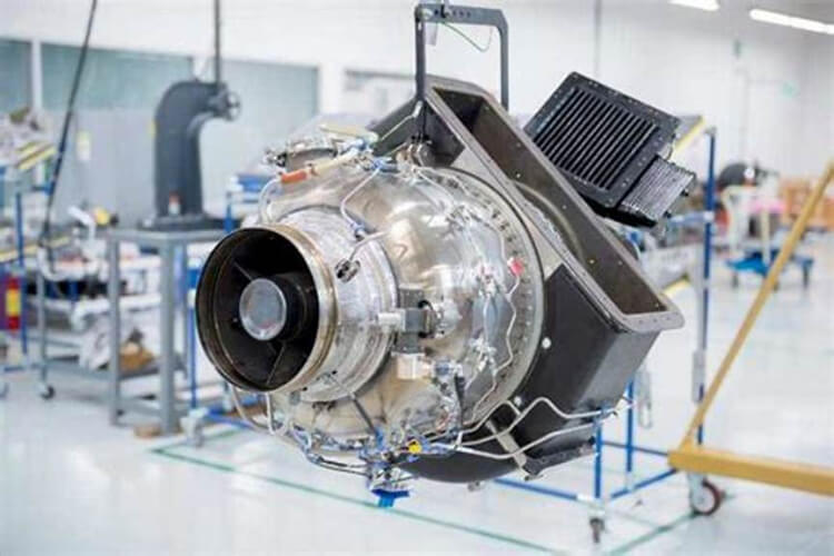

GaN wafers are becoming increasingly important in various high-tech applications due to their superior electronic properties.

Integration in Consumer Electronics:
GaN on Sapphire is expected to play a larger role in consumer electronics, leading to the development of smaller, more efficient devices in areas such as smartphones, laptops, and wearables.
Continued Expansion in 5G Infrastructure:
With the global rollout of 5G networks, the demand for GaN on Sapphire is expected to surge, driving further innovation in RF power amplifiers and high-frequency devices.
Emergence in Quantum Computing:
GaN on Sapphire’s unique properties may find applications in emerging technologies, including quantum computing, where its reliability and efficiency can contribute to the development of advanced computing systems.
In conclusion, GaN on Sapphire stands at the forefront of semiconductor technology, offering a potent combination of gallium nitride’s electrical prowess and sapphire’s substrate advantages. Its impact spans diverse industries, from telecommunications to automotive and beyond. As the demand for high-frequency, efficient, and reliable semiconductor devices continues to rise, GaN on Sapphire is poised to play a pivotal role in shaping the future of electronic systems and technologies.
Compared to traditional silicon, constructing GaN devices on sapphire allows for a much higher operating voltage due to sapphire’s better insulating properties, critical for emerging EV and three-phase power applications
XINKEHUI GaN on Sapphire sizes include 4 inch, 6 inch, 8 inch, 12 inch.
LEDs and light-emitting diodes. GaN is found on Silicon, SiC, and InGaN substrates. These substrates offer several advantages when it comes to designing and manufacturing LEDs.
1. Advanced Manufacturing Techniques
Epitaxial Growth: XinKehui might use advanced epitaxial growth techniques, such as Metal-Organic Chemical Vapor Deposition (MOCVD) or Hydride Vapor Phase Epitaxy (HVPE), which are crucial for producing high-quality GaN wafers.
Precise Control: The company likely employs precise control over the growth conditions, ensuring uniformity and reducing defects in the crystal structure.
2. High-Quality Material
Low Defect Density: By utilizing cutting-edge production technologies, XinKehui can produce GaN wafers with low defect densities, which is critical for high-performance electronic and optoelectronic devices.
Purity: Ensuring high purity of the GaN material is essential for achieving optimal electrical properties.
3. Innovation in Substrate Technology
Substrate Materials: XinKehui might innovate in the choice of substrates, such as using silicon, sapphire, or silicon carbide, depending on the application requirements. Each substrate has its own set of advantages in terms of cost, thermal conductivity, and lattice matching.
Stress Management: Techniques to manage and reduce stress between the GaN layer and the substrate can improve wafer quality and longevity.
4. Scalability and Cost Efficiency
Large-Scale Production: XinKehui may have the capability to produce GaN wafers at a large scale, which can reduce costs and improve accessibility for various industries.
Economies of Scale: Leveraging economies of scale can make their GaN wafers more cost-effective compared to competitors.
5. Customization and Flexibility
Tailored Solutions: The company might offer customized GaN wafer solutions tailored to specific customer requirements, whether for power electronics, RF devices, LEDs, or other applications.
Flexible Production Processes: Adaptability in their production processes allows XinKehui to quickly respond to market demands and technological advancements.
6. Research and Development
Continuous Improvement: An emphasis on R&D ensures that XinKehui stays at the forefront of GaN technology, continuously improving wafer quality and developing new applications.
Collaboration with Academia and Industry: Partnerships with research institutions and industry players can foster innovation and accelerate the development of new technologies.
7. Quality Assurance
Rigorous Testing: Implementing stringent quality assurance processes ensures that each wafer meets high standards for performance and reliability.
Certification and Compliance: Adherence to international standards and certifications can enhance trust and credibility among customers.
8. Environmental and Sustainability Practices
Eco-Friendly Processes: XinKehui might adopt environmentally friendly manufacturing processes, reducing the environmental impact of GaN wafer production.
Energy Efficiency: Efficient use of energy and resources in their production facilities can contribute to sustainability and cost savings.