Table of contents
BSOI (Bonded Silicon-On-Insulator) wafers are advanced semiconductor substrates used in the fabrication of high-performance and low-power integrated circuits. These wafers are designed to improve the efficiency and capabilities of electronic devices by utilizing a unique structure that includes a silicon layer bonded to an insulating layer.

Silicon Layer: This is the topmost layer where active devices are fabricated. It provides a high-quality, crystalline surface for the creation of transistors and other components.
Buried Oxide (BOX) Layer: Below the silicon layer is the buried oxide layer, typically made of silicon dioxide (SiO₂). This insulating layer electrically isolates the silicon layer from the underlying substrate, reducing parasitic capacitance and leakage currents.
Silicon Substrate: The base layer that provides mechanical support to the entire structure. This layer is usually a thick silicon wafer.
1. Reduced Power Consumption: The insulating BOX layer minimizes leakage currents, which helps in reducing the overall power consumption of the devices.
2. Enhanced Performance: BSOI wafers reduce parasitic capacitance, which leads to faster switching speeds and improved device performance.
3. Better Thermal Management: The BOX layer helps in thermal isolation, which enhances the thermal management of the devices, allowing them to operate efficiently at higher temperatures.
4. Improved Device Scaling: BSOI technology facilitates further miniaturization of electronic components, supporting the ongoing trend towards smaller and more powerful electronic devices.
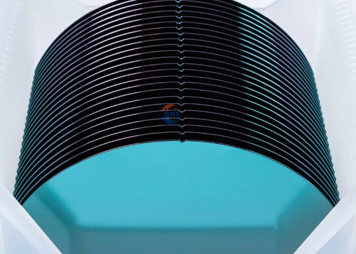
1. High-Performance Processors: BSOI wafers are commonly used in the manufacturing of high-performance processors for computing and mobile devices due to their ability to improve speed and reduce power consumption.
2. Radio Frequency (RF) and Analog Circuits: These wafers are ideal for RF and analog circuits, providing better noise performance and linearity.
3. Sensors and MEMS: BSOI technology is also used in the production of high-precision sensors and Micro-Electro-Mechanical Systems (MEMS), benefiting from its excellent electrical isolation and mechanical properties.
The creation of BSOI wafers involves several key steps:
1. Oxidation: A thin layer of silicon dioxide is grown or deposited on a silicon wafer.
2.Bonding: Another silicon wafer is bonded to the oxidized surface, creating a sandwich structure.
3. Thinning: The top silicon wafer is then thinned down to the desired thickness using techniques such as grinding, polishing, and etching.
4. Annealing: The bonded wafers are annealed to strengthen the bond and improve the quality of the buried oxide layer.
BSOI wafers represent a critical advancement in semiconductor technology, enabling the development of faster, more efficient, and lower-power electronic devices. Their unique structure and properties make them an essential component in modern electronics, driving innovations in various fields.
| Growth method | Cz, MCz, A-MCz® |
| Diameter | 150 mm, 200 mm |
| Crystal orientation | <100>, <110>,<111> |
| N type dopants | Antimony, Phosphorus |
| P type dopants | Boron |
| Resistivity | From <0.001 to >7,000 Ohm-cm* *Resistivity range varies by dopant and orientation |
| Device layer thickness | From 1 μm to >200 μm Tolerance ±0.5 μm (standard BSOI), ±0.3 μm (0.3 SOI), ±0.1 μm (E-SOI®, Power Management SOI), ±0.5 μm or lower (C-SOI®) |
| Buried oxide layer thickness | From 0.3 μm to 4 μm, typically between 0.5 μm and 2 μm Type: thermal oxide |
| Handle wafer thickness | 200 mm: 300 μm to 950 μm, typically 725 μm 150 mm: 300 μm to 950 μm, typically 380 μm |
| Back surface | Polished or etched |
| Terrace area | Standard or Terrace Free (Available for 200 mm BSOI, E-SOI®and Power Management SOI) |
BSOI (Bonded Silicon-On-Insulator) wafers are transformative in the semiconductor industry, enabling more ambitious device designs while maintaining cost-effectiveness. Here’s how BSOI wafers achieve this:
1. Enhanced Performance at Lower Costs
(1) High Speed and Low Power Consumption: Reduced Parasitic Capacitance: The buried oxide (BOX) layer in BSOI wafers minimizes parasitic capacitance, leading to faster switching speeds.
(2) Lower Power Leakage: The insulating properties of the BOX layer significantly reduce power leakage, resulting in lower overall power consumption. This is particularly beneficial for battery-powered devices, extending battery life.
(3) Scalability: Device Miniaturization: BSOI technology supports the continued miniaturization of electronic components, allowing more functionality to be packed into smaller spaces without a proportional increase in cost.
2. Improved Thermal Management
(1) Thermal Isolation: The BOX layer provides effective thermal isolation, which improves heat dissipation and allows devices to operate at higher speeds without overheating. This leads to better performance and reliability, reducing the need for costly cooling solutions.
3. Cost-Effective Manufacturing
(1) Simplified Fabrication Process: Integration and Yield: BSOI wafers simplify the integration of complex device architectures, improving yield rates during manufacturing. Higher yields translate to lower costs per chip.
(2) Compatibility with Existing Infrastructure: BSOI wafers can be processed using existing semiconductor fabrication equipment, minimizing the need for significant capital investment in new tools or processes.
4. Versatility in Applications
Diverse Use Cases:
(1) High-Performance Computing: BSOI wafers are ideal for high-performance processors used in computers, servers, and mobile devices, delivering superior speed and energy efficiency.
(2) RF and Analog Applications: The low noise and high linearity of BSOI wafers make them suitable for RF and analog circuits, which are crucial in telecommunications and IoT devices.
(3) Sensors and MEMS: BSOI technology enhances the precision and reliability of sensors and MEMS, which are widely used in automotive, healthcare, and industrial applications.
5. Reliability and Longevity
(1) Enhanced Device Longevity: The reduced power consumption and improved thermal management contribute to the longevity of devices made with BSOI wafers. This reliability reduces the total cost of ownership, making BSOI-based devices more cost-effective over their lifespan.
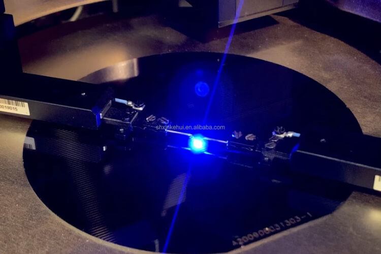
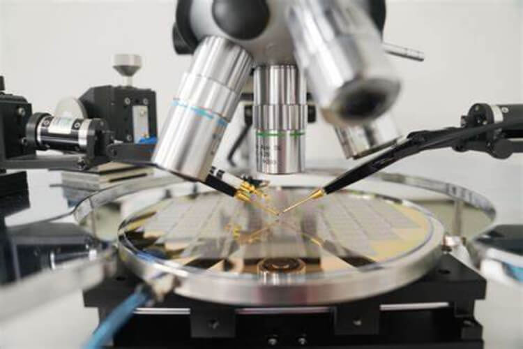
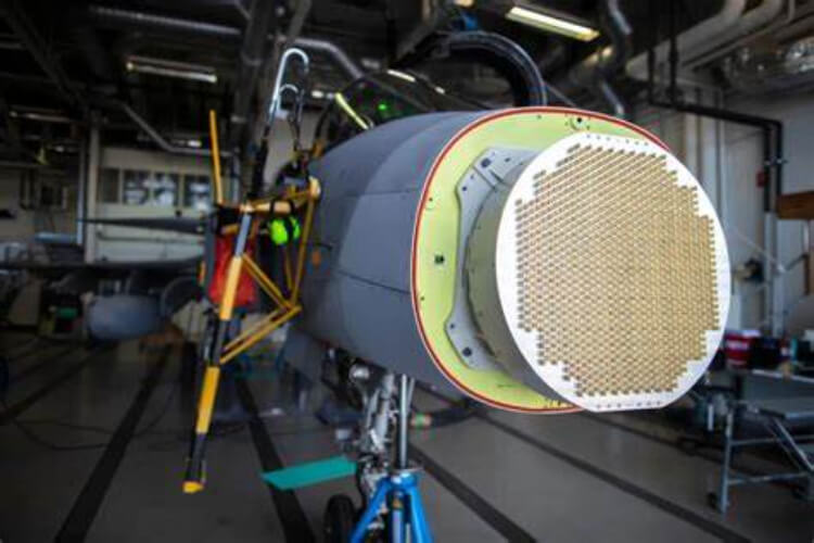
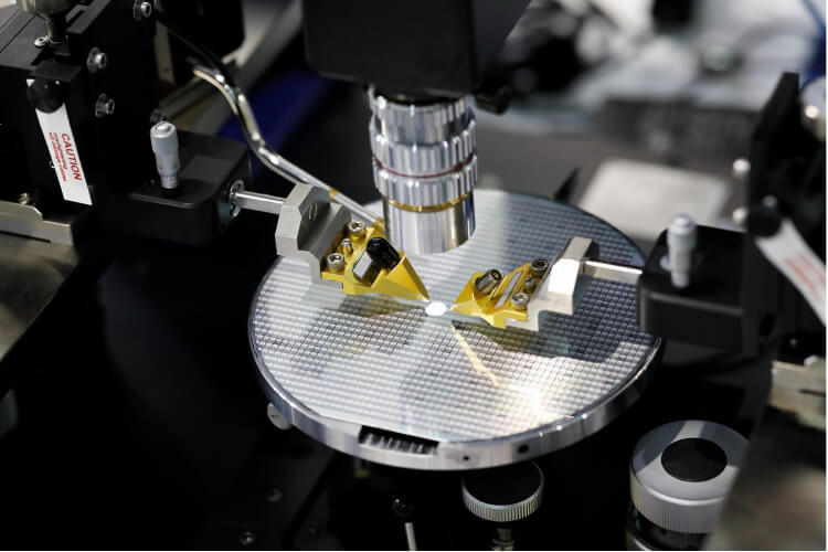
BSOI wafer is an advanced solution with multiple benefits:
BSOI variations for specialized needs:
Xinkehui 0.3 SOI is a bonded Silicon On Insulator wafer, which has buried oxide (BOX) layer between a bottom handle wafer and a top silicon wafer that is thinned with extra precision to achieve improved ±0.3 μm device layer thickness tolerance. This improved device uniformity is a relatively cost-effective solution enabling improved device performance and precision and additional freedom to device design. Even higher uniformity can be achieved with Xinkehui E-SOI® wafers. The 0.3 SOI wafer is beneficial platform for many MEMS devices such as pressure sensors and resonators.
Xinkehui DSOI is a bonded Silicon On Insulator wafer, that has two device and buried oxide layers with different thicknesses. The D-SOI wafer is beneficial platform for MEMS and photonics devices.
Xinkehui LSOI is a bonded Silicon On Insulator wafer combining thick and highly doped device layer. This kind of Low Resistivity Bonded SOI wafer is beneficial in certain MEMS devices eg. silicon oscillators as no external packaging is needed unlike with quartz-based oscillators. This leads to reduced board size an absence of quality issues with external chips.
Xinkehui Thick SOI is a bonded Silicon On Insulator wafer with very thick device layer. The bonding process enables the manufacture of very thick, over 200 μm SOI device layers that would not be possible with other competing technologies.
Xinkehui has the following advantages in processing BSOI (Bonded Silicon on Insulator) Wafer:
1. High-precision processing: Xinkehui uses advanced equipment and technology to achieve high-precision processing. This is especially important for the production of BSOI Wafer, because the BSOI structure requires very precise control.
2. High-quality materials: Xinkehui uses high-quality silicon wafers and oxide materials to ensure the high performance and reliability of the final product.
3. Efficient production: Xinkehui has an automated production line and an efficient production process, which can quickly respond to customer needs and shorten delivery cycles.
4. Technical support: Xinkehui has a professional technical team that can provide customers with comprehensive technical support and solutions to help customers solve various problems encountered in the processing of BSOI Wafer.
5. Innovation ability: Xinkehui continues to carry out technological innovation and research and development, and is committed to improving the performance of BSOI Wafer and reducing production costs.
6. Reliable quality control: Xinkehui implements a strict quality control system, with strict testing and control in every link from raw material procurement to production and manufacturing to ensure the stability and reliability of product quality.

These advantages enable Xinkehui to maintain competitiveness in the field of BSOI Wafer processing and provide customers with high-quality products and services.
In addition to BSOI wafers, we can also provide you with many other optical products. We look forward to your consultation.