Table of contents
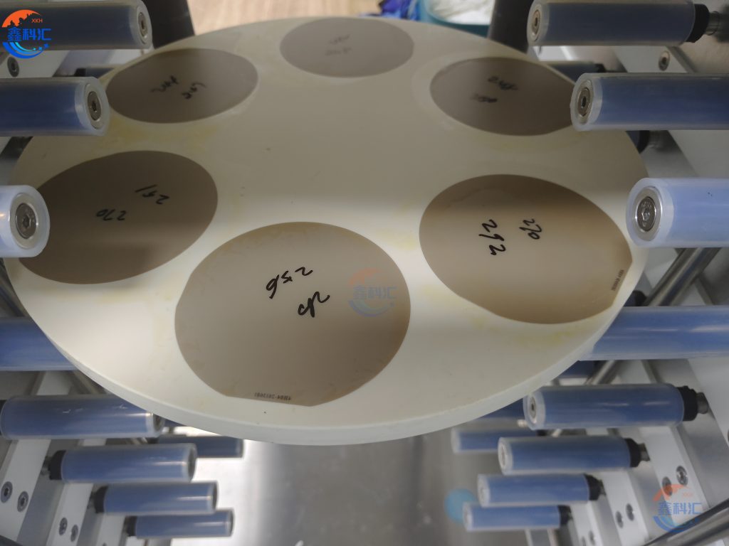
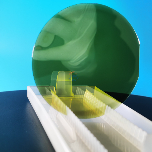
The customer is a trading company in Shenzhen, China. Their main export country is Russia. This time, their end customer needs 100 pieces of 3 inch silicon carbide (SIC) wafers.
The supplier that the customer cooperated with before could only provide him with regular sizes of silicon carbide (SIC) wafers, and could not provide him with 3 inch silicon carbide (SIC) wafers customized services. Therefore, he had to find a new cooperative manufacturer.
The customer contacted us through our official website. Our sales learned from the communication with the customer that:The customer needs 4H-SIC P grade or N grade. A 3 inch silicon carbide (SIC) wafers product with a thickness of 350um with a laser mark on the back.
According to customer needs and combined with some of our previous processing and production experience, under the premise that the customer has no special mandatory needs, we recommend P-grade 4H-SIC to the customer because the cost of P grade is relatively low, which is more cost-effective for customers, and the yield rate is better.
The customer was very satisfied with the solution and price we proposed and placed an order with me.
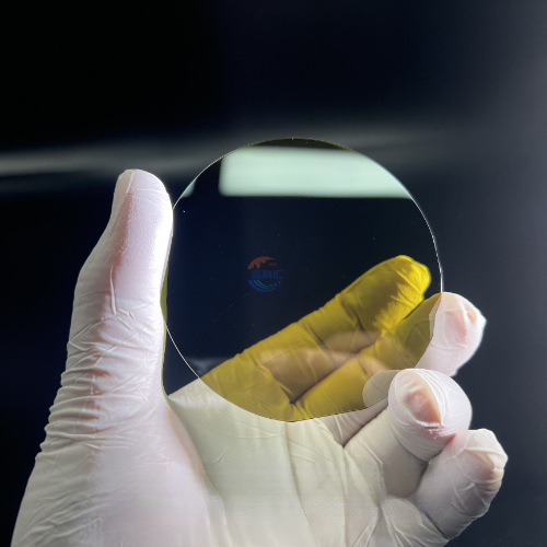
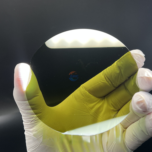
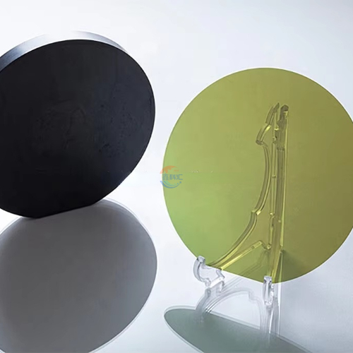
We can provide you with 3 inch silicon carbide (SIC) wafers with the following parameters. If you want to know more information, please feel free to contact us. Looking forward to your message.
| Product Performance | P Grade | N Grade | |
| Crystal Parameter | |||
| Crystal form | 4H | ||
| Polymorphic | Not allow | Area ≤5% | |
| < strong>Microtubule density | ≤0.5 pc /cm² | ≤0.5 pc/cm² | |
| Hexagonal void | Not allow | Area ≤5% | |
| Hexagonal surface mixed crystal | Not allow | Area ≤5% | |
| Wrapper | Area ≤0.05% | N/A | |
| Specific resistance | ≥1E9Ω•cm | ≥1E5Ω•cm | |
| (0004) XRD Swing Curve half-height Width (FWHM) | ≤45 Arcseconds | N/A | |
| Mechanical parameter | |||
| Diameter | 76.2 mm±0.38 mm | ||
| Surface orientation | {0001}±0.2° | ||
| Main reference edge length | 22.0 mm ± 2.0 mm | ||
| Main reference edge length | 22.0 mm ± 2.0 mm | ||
| Secondary reference side length | 11.0 mm ± 1.5 mm | ||
| Principal reference plane orientation | Parallel to <11-20> ± 5.0˚ | ||
| Secondary reference plane orientation | Clockwise to the main reference plane at 90˚ ± 5.0˚, Si facing up | ||
| Surface treatment | C-side: Mirror polishing, SI-Side: Chemical Mechanical Polishing (CMP) | ||
| Wafer edge | Chamfer | ||
| Surface roughness (5μm×5μm) | Si surface Ra<0.2 nm | ||
| Thickness | 350.0±25.0μm or 500.0±25.0μm | ||
| LTV(10mm×10mm) | ≤3µm | ≤5µm | |
| LTV(10mm×10mm) | ≤3µm | ≤5µm | |
| Total thickness variation(TTV) | ≤10µm | ≤10µm | |
| Curvature (absolute value)(Bow) | ≤15µm | ≤25µm | |
| Warp | ≤25µm | ≤35µm | |
| Curvature (absolute value)(Bow) | ≤15µm | ≤25µm | |
| Surface parameters | |||
| Edge breakage/gap | No edge breakage with length or width ≥0.5mm is allowed | ≤2, and each length and width ≤1.0mm | |
| Scratch (Si surface,CS8520) | ≤4 pieces, and the total length ≤0.5 times the diameter | ≤5 pieces, and the total length ≤1.5 times the diameter | |
| Crack | Not allow | ||
| Contamination | Not allow | ||
| Edge removal | 3mm | ||
Silicon carbide (SIC) wafers are crucial in various high-power, high-frequency, and high-temperature applications due to their exceptional properties. Here’s a detailed look at 3 inch SIC wafers:
Diameter: 3 inches (76.2 mm)
Thickness: Typically ranges from 250 µm to 500 µm
Orientation: Common orientations include 4° off-axis (0001) and (0001) substrates
Surface Finish: Epi-ready wafers typically have a polished surface on one side and a ground surface on the other.
Power Electronics: SiC wafers are used in the production of power semiconductor devices like MOSFETs, diodes, and power modules.
High-Frequency Electronics: The high electron mobility in SiC makes it suitable for high-frequency applications like RF amplifiers.
High-Temperature Electronics: SiC devices can operate at higher temperatures compared to silicon devices, making them suitable for aerospace, automotive, and industrial applications.
LEDs and Lighting: SiC wafers serve as substrates for the growth of gallium nitride (GaN) for LED production.


Silicon Carbide (SIC) Wafers are integral to the advancement of modern electronics, especially in areas where performance, efficiency, and durability are paramount. Their adoption continues to grow as manufacturing processes improve and costs decrease.
Xinkehui, as a silicon carbide (SiC) manufacturer, might have several advantages contributing:
1. Advanced Manufacturing Processes: Xinkehui might employ cutting-edge techniques for crystal growth and wafer fabrication, ensuring high-quality and high-purity SiC wafers.
2. Innovative R&D: Continuous research and development efforts could lead to innovative products and processes, enhancing performance and reducing costs.
3. High-Quality Products: Emphasis on stringent quality control measures ensures the production of defect-free and reliable SiC wafers.
4. Large-Scale Production: Xinkehui’s ability to produce SiC wafers at a large scale can meet the growing demand from various industries.
5. Cost Efficiency: Economies of scale and efficient production processes may result in competitive pricing.
6. Tailored Solutions: Offering customization in terms of wafer specifications, doping levels, and surface finishes to meet specific customer requirements.
7. Flexible Production: Ability to adapt to changing market demands and technological advancements.
8. Technical Support: Providing comprehensive technical support to help customers integrate SiC wafers into their applications.
9. After-Sales Service: Ensuring robust after-sales service and support to address any issues and maintain customer satisfaction.
10.Collaborations with Industry Leaders: Partnerships with key players in the semiconductor and electronics industries can enhance technological capabilities and market reach.
