Table of contents
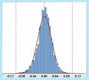
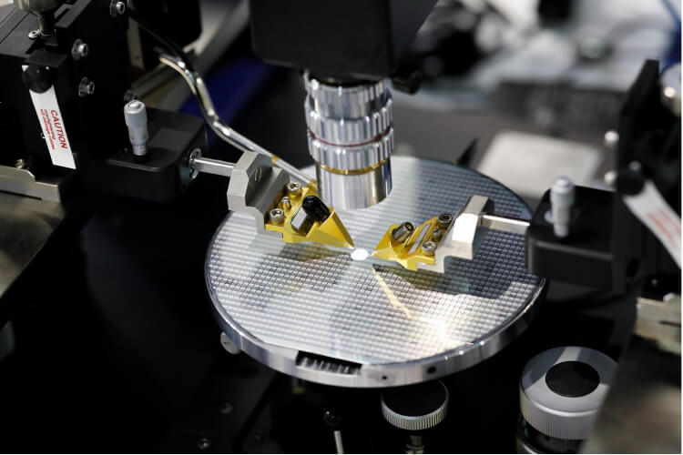
E-SOI wafers are enhanced bonded silicon-on-insulator wafers with a buried oxide (BOX) layer between the bottom handle wafer and the top silicon wafer that is thinned with extremely high precision to achieve best-in-class device layer thickness uniformity. The device layer of Enhanced SOI (E-SOI) wafers can be made thicker and more uniform than competing SOI technologies.

Typically MEMS sensors are built on the device layer whilst the buried oxide (BOX) is an excellent electric insulating layer and an effective etch stop. The BOX layer can also act as a sacrificial layer for complex components and released structures. The handle wafer supports the structure, but can also be utilized in sealing the structure or as part of the sensing element.
An E-SOI (Enhanced Silicon-On-Insulator) wafer is a specialized type of semiconductor substrate that offers several advantages in the manufacturing of integrated circuits (ICs). These advantages include:
1. Reduced Power Consumption
E-SOI wafers allow for lower power consumption in ICs because the insulating layer (typically silicon dioxide) reduces leakage currents. This is particularly important in mobile and battery-operated devices.
2. Improved Performance
The reduced parasitic capacitance in E-SOI wafers enhances the speed of the transistors, leading to faster circuit operation. This makes E-SOI wafers suitable for high-speed applications.
3. Better Heat Dissipation
The insulating layer in E-SOI wafers helps in better thermal management, reducing the heat generated by the circuits. This is crucial for maintaining performance and reliability in high-density ICs.
4. Lower Substrate Noise
E-SOI wafers exhibit lower substrate noise due to the isolation provided by the buried oxide layer. This is beneficial for analog and mixed-signal circuits where noise can degrade performance.
5. Scalability and Integration
E-SOI technology supports the scaling down of transistors, allowing for the creation of smaller, more densely packed circuits. It also facilitates the integration of different types of devices (e.g., analog, RF, digital) on the same chip.
6. Radiation Hardness
E-SOI wafers are more resistant to radiation-induced soft errors, making them suitable for applications in space, military, and other high-radiation environments.
7. Enhanced Design Flexibility
The E-SOI structure provides more flexibility in circuit design, enabling the implementation of advanced features like dynamic threshold voltage adjustment, which can optimize performance and power consumption dynamically.
8. Reduced Short Channel Effects
The insulating layer in E-SOI wafers mitigates short channel effects, which are prevalent in very small transistors. This contributes to maintaining the integrity and performance of the transistors as they are scaled down.
9. Lower Parasitic Capacitance
The SOI structure helps in reducing the parasitic capacitance between the device and the substrate, leading to faster switching speeds and improved overall performance of the ICs.

E-SOI wafer is an advanced solution with multiple benefits:
1. More freedom to device design than with competing technologies
2. Improved device performance and precision
3. Reduced device size and cost
4. Improved device yield
These advantages make E-SOI wafers a valuable choice in advanced semiconductor manufacturing, particularly for applications requiring high performance, low power consumption, and high reliability.
E-SOI (Enhanced Silicon-On-Insulator) wafers are used in various applications across different sectors due to their ability to improve performance, reduce power consumption, and enhance reliability in integrated circuits (ICs). Some key applications of E-SOI wafers include:
1. Mobile Devices and Wearables
Smartphones and smartwatches benefit from E-SOI wafers due to their low power consumption and high-speed capabilities. These characteristics are crucial for extending battery life while maintaining high performance in portable electronics.
2. High-Performance Computing (HPC)
E-SOI wafers are used in microprocessors and graphic processing units (GPUs) in high-performance computing systems. The reduced parasitic capacitance and improved thermal management enable faster processing speeds and higher efficiency, which are essential in HPC environments.
3. Automotive Electronics
In the automotive industry, E-SOI wafers are utilized in advanced driver-assistance systems (ADAS), infotainment systems, and other in-car electronics. The wafers’ ability to operate reliably in high-temperature environments and their resistance to radiation-induced errors are particularly valuable in automotive applications.
4. Internet of Things (IoT)
E-SOI wafers are employed in IoT devices that require low power consumption and high performance, such as smart sensors, connected home appliances, and industrial IoT systems. The energy efficiency of E-SOI wafers is critical for devices that need to operate on small batteries for extended periods.
5. Telecommunications
E-SOI wafers are used in 5G infrastructure and networking equipment, where high speed and low power consumption are necessary. They support the integration of high-frequency components, which are essential for modern communication systems.
6. Aerospace and Defense
The radiation hardness of E-SOI wafers makes them suitable for use in satellites, spacecraft, and military electronics. These applications demand high reliability in harsh environments, where traditional silicon wafers might fail.
7. Consumer Electronics
E-SOI wafers are used in various consumer electronics, including gaming consoles, televisions, and audio systems. The enhanced performance and power efficiency contribute to better user experiences in these devices.
8. Medical Devices
In the medical field, E-SOI wafers are used in implantable devices, portable diagnostic equipment, and other medical electronics. The wafers’ low power consumption and reliability are vital for devices that need to operate continuously or in sensitive environments.
9. Mixed-Signal and RF Circuits
E-SOI wafers are ideal for mixed-signal ICs and RF (Radio Frequency) circuits, where low noise and high-frequency performance are critical. These applications include wireless communication devices and radar systems.
10. Artificial Intelligence (AI) and Machine Learning (ML)
E-SOI wafers are increasingly used in AI accelerators and ML processors. The combination of high speed, low power consumption, and scalability makes E-SOI wafers suitable for handling the intensive computational demands of AI and ML algorithms.


These applications highlight the versatility and importance of E-SOI wafers in modern electronics, particularly in areas where performance, power efficiency, and reliability are paramount.
In terms of producing E-SOI (Enhanced Silicon On Insulator) wafers, xinkehuij has the following advantages:
1. Technical capabilities
(1) Advanced process control: Mastering high-precision and stable process technology, it can meet strict specifications in terms of SOI layer thickness and uniformity.
(2) Innovation capabilities: Unique technological innovations are adopted in the production process, such as the introduction of new materials or unique manufacturing processes, which improve the electrical performance and reliability of wafers.
2. Equipment and facilities
(1) Advanced equipment: The use of cutting-edge equipment such as ion implanters, epitaxial growth equipment and chemical mechanical polishing (CMP) equipment ensures high quality and consistency of wafers.
(2) Intelligent manufacturing system: Through automated and intelligent production systems, human errors are reduced and production efficiency is improved.
3. Quality control
(1) Strict quality management system: Comprehensive quality control is implemented, from raw material procurement to finished product inspection, to ensure that every E-SOI wafer meets the high standards of customers.
(2) Real-time monitoring and feedback mechanism: Through real-time data monitoring and feedback, production parameters can be adjusted quickly to ensure product consistency and stability.
4. Cost advantage
(1) Large-scale production: With the ability to produce on a large scale, the production cost can be reduced through economies of scale.
(2) Supply chain optimization: With advantages in supply chain management, the cost of raw materials and logistics can be effectively controlled, thereby reducing the overall production cost.
5. Customer service
(1) Customized service: Able to provide customized E-SOI wafers according to the specific needs of customers to meet the needs of different application scenarios.
(2) Fast delivery: With flexible production scheduling capabilities, it can quickly respond to customer order needs and shorten the delivery cycle.
As with other Silicon On Insulator wafers, the E-SOI wafer can be customized to match your exact device and process needs. Xinkehui has the widest selection of silicon wafers in the market, and our sales and technical support are happy to help in customization and selection of wafer parameters to find an optimal solution for your needs. E-SOIwafers are also available as Terrace Free SOI wafers.
| Growth method | Cz, MCz, A-MCz |
| Diameter | 150 mm, 200 mm |
| Crystal orientations | <100>, <110>, <111> |
| N type dopants | Antimony, Phosphorus |
| P type dopants | Boron |
| Resistivity | From <0.001 to >7,000 Ohm-cm* *Resistivity range varies by dopant and orientation |
| Device layer thickness | From 1 μm to >200 μm Tolerance ±0.5 μm (standard BSOI), ±0.3 μm (0.3 SOI), ±0.1 μm (E-SOI, Power Management SOI), ±0.5 μm or lower (C-SOI) |
| Buried oxide layer thickness | From 0.3 μm to 4 μm, typically between 0.5 μm and 2 μm Type: thermal oxide |
| Handle wafer thickness | 200 mm: 300 μm to 950 μm, typically 725 μm 150 mm: 300 μm to 950 μm, typically 380 μm |
| Back surface | Polished or etched |
| Terrace area | Standard or Terrace Free (Available for 200 mm BSOI, E-SOI and Power Management SOI) |
In addition to C-SOI Wafers , we can also provide you with many other optical products. We look forward to your consultation.