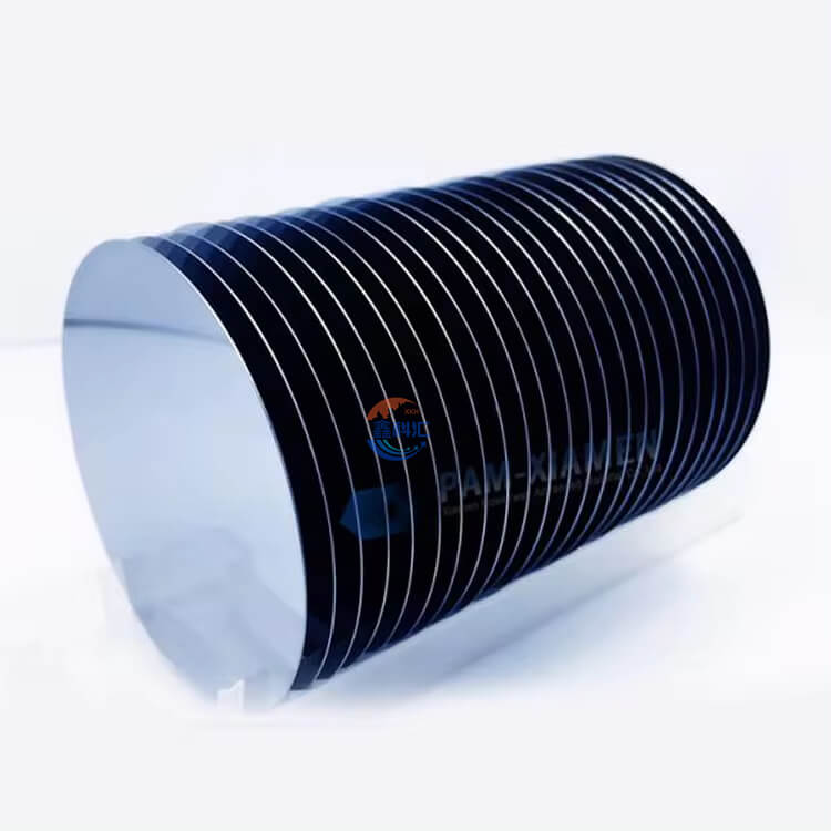
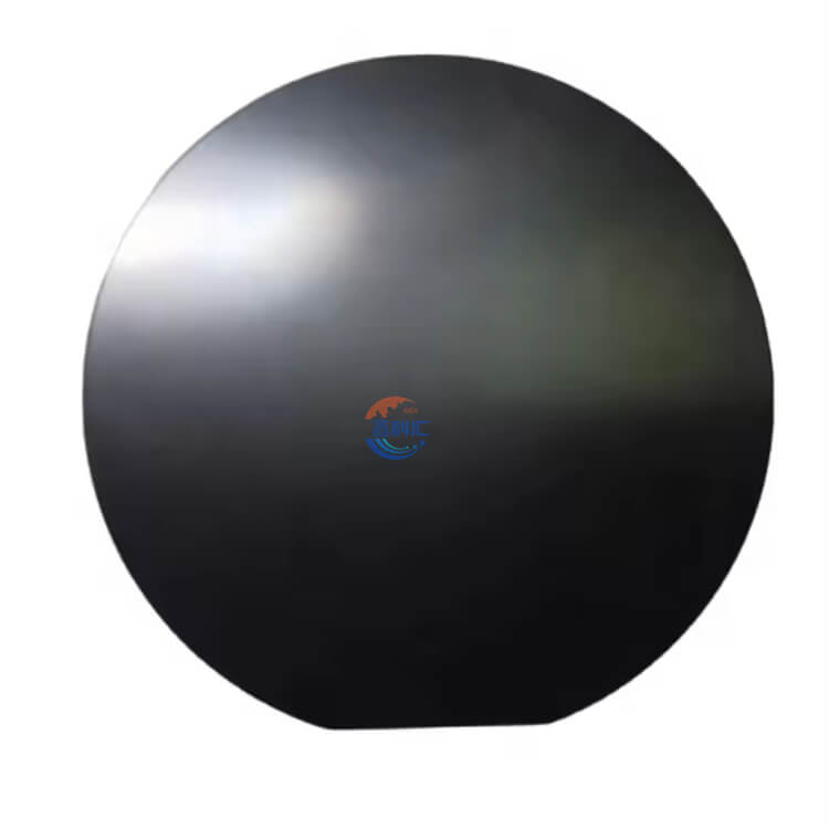
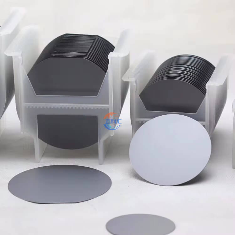
Silicon wafers have several advantages, especially in the semiconductor industry:
1. Semiconductor Fabrication: Silicon wafers are the foundational material for manufacturing integrated circuits (ICs) and other semiconductor devices. Their high purity and crystalline structure make them ideal for this purpose.
2. Electrical Properties: Silicon has excellent electrical properties, such as high carrier mobility and a stable oxide layer (silicon dioxide), which is essential for creating reliable semiconductor devices.
3. Uniformity: Silicon wafers can be manufactured with high uniformity in terms of thickness, resistivity, and crystal orientation, ensuring consistent performance across a batch of semiconductor devices.
4. Compatibility: Silicon wafers are compatible with a wide range of semiconductor processing techniques, including doping, etching, and deposition methods, making them versatile for various device fabrication processes.
5. Scaling: Silicon wafers have allowed for the scaling down of transistor sizes, enabling the continuous improvement of semiconductor devices’ performance and density (Moore’s Law).
6. Mechanical Properties: Silicon wafers are mechanically robust and can withstand the stresses associated with semiconductor processing steps like polishing, etching, and lithography.
7. Cost Efficiency: Despite being a high-tech material, silicon wafers benefit from economies of scale due to widespread use in the semiconductor industry, which helps in keeping production costs relatively low compared to other materials.


These advantages collectively contribute to silicon wafers being the material of choice for manufacturing modern semiconductor devices used in electronics, computing, and telecommunications.
Silicon wafers (Si wafers) are a basic material used in semiconductor manufacturing and have many unique physical and chemical properties. Below is a detailed description of the properties of Si wafers and their importance in the semiconductor industry.
1. Crystal structure: The silicon wafer is composed of pure silicon crystals, and its lattice structure belongs to the diamond cubic structure. Silicon atoms are joined together in covalent bonds to form a uniform crystal structure.
2. Crystal orientation: Silicon wafer usually has < 100> , < 110> < 111> Crystal orientation, which determines its specific use and performance in the manufacturing process.
3. Crystal face: The surface of a silicon wafer is usually a (100) or (111) crystal face, which has an important impact on different types of processing.
4. Size: Silicon wafers are typically 2, 4, 6, 8, or 12 inches in diameter, depending on the requirements of the final product and the limitations of the manufacturing process.
5. Thickness: The thickness of silicon wafers typically varies between a few hundred microns to several millimeters, depending on the manufacturing process and the end application.
6. Impurity content: High purity is one of the key characteristics of Si wafer Impurity levels must be kept extremely low, usually measured in parts per million (ppm).
7. Electronic structure: A silicon wafer is a semiconductor material whose electronic structure allows it to become a conductor or insulator when properly doped. The electrical conductivity of a silicon wafer depends on the type and concentration of doping.
8. Optical properties: Silicon wafers have different transmission and reflection properties for different wavelengths of light, which are critical in photolithography and other semiconductor processing.
9. Mechanical properties: The silicon wafer has excellent mechanical stability and hardness, which enables it to maintain shape stability in various processing processes.
10. Thermal characteristics: Silicon has good thermal conductivity and thermal stability, which is essential for the heat dissipation and stable operation of integrated circuits.
11. Chemical reactivity: Silicon wafers have high chemical inertness to many chemicals, but they also react with some compounds under certain conditions, which requires attention during the manufacturing process.
12. Surface treatment: The surface of Si wafer is usually subjected to a variety of treatments, such as chemical mechanical polishing (CMP), cleaning and coating, to ensure the surface’s flatness and purity.
13. Lattice defects: Silicon wafers may have lattice defects, such as dislocations and grain boundaries, that can affect the electrical and mechanical properties of the wafer.
14. Electronic mobility: The electronic mobility of silicon wafers is an important parameter when it is used in electronic devices such as transistors, which directly affects the speed and performance of the devices.
15. Photoluminescence: In some special applications, silicon wafers may exhibit photoluminescence properties, which have important implications in optoelectronics and sensor technology.
16. Crystallization method: Si wafers can be prepared by a variety of methods such as solidification, vapor deposition, and liquid phase diffusion, each of which affects the performance and cost of silicon wafers.
| Product: | Silicon (Si) wafer |
| Grade: | IC prime grade |
| Purity: | >99.999999999% (11N) |
| Dimension: | Standard dimensions:• 1” × 0.5 mm• 2” × 0.28 / 0.4 / 0.5 mm• 3” × 0.38 mm• 4” × 0.525 mm• 5” × 0.6 mm• 6” × 0.625 mm• 8” × 0.725 mm Other diameters and thicknesses available• We provide small-scale non-standard wafers for research / testing purposes. |
| Orientation: | <100> / <110> / <111> / off-axis / others |
| Conductive type: | • Undoped (also called intrinsic, native) type• N-type: phosphor (P) doped• P-type: boron (B) doped |
| Resistivity: | Standard resistivity for undoped wafers:• 3000 – 6000 Ω·cm Standard resistivity for n-/ p-type wafers:• 0.001 – 0.009 Ω·cm• 1 – 10 Ω·cm• 10 – 20 Ω·cm• 90 – 100 Ω·cm Other resistivity available |
| Polishing: | • As-cut wafers without polishing• Single side epi-polished• Double side epi-polished |
| Surface roughness: | < 0.5 nm |
| Remarks: | Si wafer with functional layers available (thermal oxide SiO2, silicon nitride Si3N4, etc) |